MAX78002EVKIT
Overview
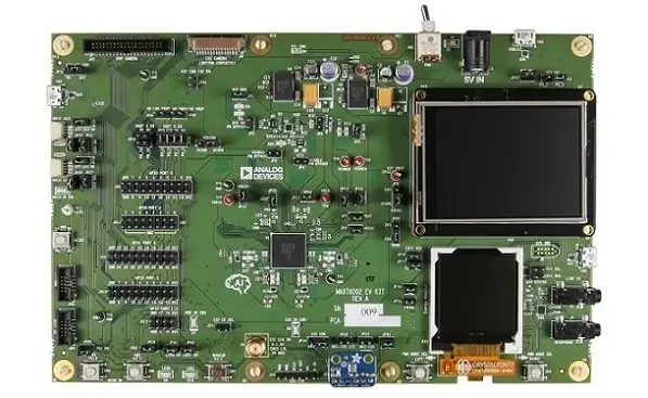
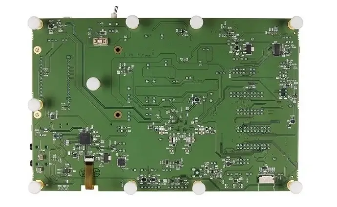
The MAX78002 evaluation kit (EV kit) provides a platform and tools for leveraging device capabilities to build new generations of artificial intelligence (AI) products.
The kit provides optimal versatility with a modular peripheral architecture, allowing a variety of input and output devices to be remotely located. DVP and CSI cameras, I2S audio peripherals, digital microphones, and analog sensors are supported, while a pair of industry-standard QWIIC connectors supports a large and growing array of aftermarket development boards. An onboard stereo audio codec offers line-level audio input and output, and tactile input is provided by a touch-enabled 2.4in TFT display. The MAX78002 energy consumption is tracked by a power accumulator, with four channels of formatted results presented on a secondary TFT display. All device GPIOs are accessible on 0.1in pin headers. A standard coaxial power jack serves as power input, using the included 5V, 3A wall-mount adapter. Two USB connectors provide serial access to the MAX78002, one directly and the other through a USB to UART bridge. A third USB connector allows access to the MAX78002 energy consumption data. Rounding out the features, a microSD connector provides the capability for inexpensive highdensity portable data storage.
The Zephyr port is running on the MAX78002 MCU.


Hardware
MAX78002 MCU:
Dual-Core, Low-Power Microcontroller
Arm Cortex-M4 Processor with FPU up to 120MHz
2.5MB Flash, 64KB ROM, and 384KB SRAM
Optimized Performance with 16KB Instruction Cache
Optional Error Correction Code (ECC SEC-DED) for SRAM
32-Bit RISC-V Coprocessor up to 60MHz
Up to 60 General-Purpose I/O Pins
MIPI Camera Serial Interface 2 (MIPI CSI-2) Controller V2.1
Support for Two Data Lanes
12-Bit Parallel Camera Interface
I2S Controller/Target for Digital Audio Interface
Secure Digital Interface Supports SD 3.0/SDIO 3.0/eMMC 4.51
Convolutional Neural Network (CNN) Accelerator
Highly Optimized for Deep CNNs
2 Million 8-Bit Weight Capacity with 1-, 2-, 4-, and 8-bit Weights
1.3MB CNN Data Memory
Programmable Input Image Size up to 2048 x 2048 Pixels
Programmable Network Depth up to 128 Layers
Programmable per Layer Network Channel Widths up to 1024 Channels
1- and 2-Dimensional Convolution Processing
Capable of Processing VGA Images at 30fps
Power Management for Extending Battery Life
Integrated Single-Inductor Multiple-Output (SIMO) Switch-Mode Power Supply (SMPS)
2.85V to 3.6V Supply Voltage Range
Support of Optional External Auxiliary CNN Power Supply
Dynamic Voltage Scaling Minimizes Active Core Power Consumption
23.9μA/MHz While Loop Execution at 3.3V from Cache (CM4 only)
Selectable SRAM Retention in Low-Power Modes with Real-Time Clock (RTC) Enabled
Security and Integrity
Available Secure Boot
AES 128/192/256 Hardware Acceleration Engine
True Random Number Generator (TRNG) Seed Generator
External devices connected to the MAX78002 EVKIT:
Color TFT Display
Audio Stereo Codec Interface
Digital Microphone
A 8Mb QSPI ram
Supported Features
The max78002evkit board supports the hardware features listed below.
- on-chip / on-board
- Feature integrated in the SoC / present on the board.
- 2 / 2
-
Number of instances that are enabled / disabled.
Click on the label to see the first instance of this feature in the board/SoC DTS files. -
vnd,foo -
Compatible string for the Devicetree binding matching the feature.
Click on the link to view the binding documentation.
max78002evkit/max78002/m4 target
Type |
Location |
Description |
Compatible |
|---|---|---|---|
CPU |
on-chip |
ARM Cortex-M4F CPU1 |
|
on-chip |
MAX32 RV32 core1 |
||
ADC |
on-chip |
ADI MAX32 ADC SAR1 |
|
Clock control |
on-chip |
||
on-chip |
MAX32 Global Control1 |
||
Counter |
on-chip |
ADI MAX32 counter6 |
|
on-chip |
ADI MAX32 compatible Counter RTC1 |
||
on-chip |
ADI MAX32 Wake-Up Timer is a unique instance of a 32-bit timer that can wake up the device from sleep, standby and backup modes1 |
||
DMA |
on-chip |
ADI MAX32 DMA1 |
|
Flash controller |
on-chip |
MAX32XXX flash controller1 |
|
GPIO & Headers |
on-chip |
MAX32 GPIO4 |
|
I2C |
on-chip |
||
Input |
on-board |
Group of GPIO-bound input keys1 |
|
Interrupt controller |
on-chip |
ARMv7-M NVIC (Nested Vectored Interrupt Controller)1 |
|
LED |
on-board |
Group of GPIO-controlled LEDs1 |
|
Mailbox |
on-chip |
ADI MAX32 SEMA Mailbox1 |
|
MTD |
on-chip |
Flash node1 |
|
Pin control |
on-chip |
MAX32 Pin Controller1 |
|
PWM |
on-chip |
ADI MAX32 PWM6 |
|
RNG |
on-chip |
ADI MAX32XXX TRNG1 |
|
Serial controller |
on-chip |
||
SPI |
on-chip |
||
SRAM |
on-chip |
Generic on-chip SRAM7 |
|
Timer |
on-chip |
ADI MAX32 timer7 |
|
on-chip |
ARMv7-M System Tick1 |
||
1-Wire |
on-chip |
ADI MAX32xxx MCUs 1-Wire Master1 |
|
Watchdog |
on-chip |
max78002evkit/max78002/rv32 target
Type |
Location |
Description |
Compatible |
|---|---|---|---|
CPU |
on-chip |
MAX32 RV32 core1 |
|
ADC |
on-chip |
ADI MAX32 ADC SAR1 |
|
Clock control |
on-chip |
||
on-chip |
MAX32 Global Control1 |
||
Counter |
on-chip |
ADI MAX32 counter6 |
|
on-chip |
ADI MAX32 compatible Counter RTC1 |
||
on-chip |
ADI MAX32 Wake-Up Timer is a unique instance of a 32-bit timer that can wake up the device from sleep, standby and backup modes1 |
||
DMA |
on-chip |
ADI MAX32 DMA1 |
|
Flash controller |
on-chip |
MAX32XXX flash controller1 |
|
GPIO & Headers |
on-chip |
MAX32 GPIO4 |
|
I2C |
on-chip |
||
Input |
on-board |
Group of GPIO-bound input keys1 |
|
Interrupt controller |
on-chip |
MAX32 RV32 Core Interrupt Controller1 |
|
LED |
on-board |
Group of GPIO-controlled LEDs1 |
|
Mailbox |
on-chip |
ADI MAX32 SEMA Mailbox1 |
|
MTD |
on-chip |
Flash node1 |
|
Pin control |
on-chip |
MAX32 Pin Controller1 |
|
PWM |
on-chip |
ADI MAX32 PWM6 |
|
RNG |
on-chip |
ADI MAX32XXX TRNG1 |
|
Serial controller |
on-chip |
||
SPI |
on-chip |
ADI MAX32 SPI1 |
|
SRAM |
on-chip |
Generic on-chip SRAM5 |
|
Timer |
on-chip |
ADI MAX32 timer6 |
|
on-chip |
ADI MAX32 RV32 system timer1 |
||
1-Wire |
on-chip |
ADI MAX32xxx MCUs 1-Wire Master1 |
|
Watchdog |
on-chip |
MAX32XXX watchdog2 |
Connections and IOs
Name |
Name |
Settings |
Description |
||||
|---|---|---|---|---|---|---|---|
JP1 |
3V3 MON |
|
|
||||
JP2 |
3V3 SW PM BYPASS |
|
|
||||
JP3 |
CNN MON |
|
|
||||
JP4 |
VCOREA PM BYPASS |
|
|
||||
JP5 |
VCOREB PM BYPASS |
|
|
||||
JP6 |
VREGO_A PM BYPASS |
|
|
||||
JP7 |
VBAT |
|
|
||||
JP8 |
VREGI |
|
|
||||
JP9 |
VREGI/VBAT |
|
|
||||
JP10 |
VDDIOH |
|
|
||||
JP11 |
VDDA |
|
|
||||
JP12 |
VDDIO |
|
|
||||
JP13 |
VCOREB |
|
|
||||
JP14 |
VCOREA |
|
|
||||
JP15 |
VREF |
|
|
||||
JP16 |
I2C1 SDA |
|
|
||||
JP17 |
I2C1 SCL |
|
|
||||
JP18 |
TRIG1 |
|
|
||||
JP19 |
TRIG2 |
|
|
||||
JP20 |
UART0 EN |
|
|
||||
JP21 |
I2C0_SDA |
|
|
||||
JP22 |
I2C0_SCL |
|
|
||||
JP23 |
UART1 EN |
|
|
||||
JP24 |
EXT I2C0 EN |
|
|
||||
JP25 |
PB1 PU |
|
|
||||
JP26 |
PB2 PU |
|
|
||||
JP27 |
I2C2 SDA |
|
|
||||
JP28 |
I2C2 SCL |
|
|
||||
JP29 |
VDDB |
|
|
||||
JP30 |
EXT I2C2 EN |
|
|
||||
JP31 |
L/R SEL |
|
|
||||
JP32 |
MIC-I2S I/O |
|
|
||||
JP33 |
MIC-I2S/CODEC |
|
|
||||
JP34 |
I2S VDD |
|
|
||||
JP35 |
I2C1 SDA |
|
|
||||
JP36 |
I2C1 SCL |
|
|
||||
JP37 |
I2S CK SEL |
|
|
||||
JP38 |
DVP CAM PWR |
|
|
||||
JP39 |
SW CAM PWUP |
|
|
||||
JP40 |
HW PWUP / SW PWUP |
|
|
||||
JP41 |
CSI CAM I2C EN |
|
|
||||
JP42 |
TFT DC |
|
|
||||
JP43 |
TFT CS |
|
|
||||
JP44 |
LED1 EN |
|
|
||||
JP45 |
LED2 EN |
|
|
Programming and Debugging
The max78002evkit board supports the runners and associated west commands listed below.
| flash | debug | debugserver | reset | rtt | attach | |
|---|---|---|---|---|---|---|
| jlink | ✅ | ✅ | ✅ | ✅ | ✅ | ✅ |
| openocd | ✅ (default) | ✅ (default) | ✅ | ✅ | ✅ |
Flashing
The MAX78002 MCU can be flashed by connecting an external debug probe to the SWD port. SWD debug can be accessed through the Cortex 10-pin connector, JH8. Logic levels are fixed to VDDIO (1.8V).
Once the debug probe is connected to your host computer, then you can simply run the
west flash command to write a firmware image into flash. To perform a full erase,
pass the --erase option when executing west flash.
Note
This board uses OpenOCD as the default debug interface. You can also use
a Segger J-Link with Segger’s native tooling by overriding the runner,
appending --runner jlink to your west command(s). The J-Link should
be connected to the standard 2*5 pin debug connector (JH8) using an
appropriate adapter board and cable.
Debugging
Please refer to the Flashing section and run the west debug command
instead of west flash.