MAX32672FTHR
Overview
The MAX32672FTHR is a rapid development platform that helps engineers quickly implement complex sensor solutions using the MAX32672 Arm® Cortex®-M4. The board also includes the MAX8819 PMIC for battery and power management. The form factor is a small, 0.9in by 2.6in, dual row header footprint that is compatible with Adafruit® FeatherWing peripheral expansion boards. The board includes an OLED display, a RGB indicator LED, and a user pushbutton. The MAX32672FTHR provides a power-optimized flexible platform for quick proof-ofconcepts and early software development to enhance time to market.
The Zephyr port is running on the MAX32672 MCU.
Hardware
MAX32672 MCU:
High-Efficiency Microcontroller for Low-Power High-Reliability Devices
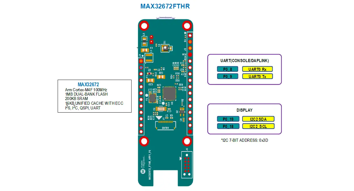
Arm Cortex-M4 Processor with FPU up to 100MHz
1MB Dual-Bank Flash with Error Correction
200KB SRAM (160KB with ECC Enabled), Optionally Preserved in Lowest Power Modes
EEPROM Emulation on Flash
16KB Unified Cache with ECC
Resource Protection Unit (RPU) and MemoryProtection Unit (MPU)
Dual- or Single-Supply Operation, 1.7V to 3.6V
Wide Operating Temperature: -40 °C to +105 °C
Flexible Clocking Schemes
Internal High-Speed 100MHz Oscillator
Internal Low-Power 7.3728MHz and Ultra-Low-Power 80kHz Oscillators
16MHz–32MHz Oscillator, 32.768kHz Oscillator(External Crystal Required)
External Clock Input for CPU, LPUART, LPTMR
Power Management Maximizes Uptime for Battery Applications
59.8μA/MHz ACTIVE at 0.9V up to 12MHz(CoreMark®)
56.6μA/MHz ACTIVE at 1.1V up to 100MHz(While(1))
3.09μA Full Memory Retention Power in BACKUPMode at VDD = 1.8V
350nA Ultra-Low-Power RTC at
Wake from LPUART or LPTMR
Optimal Peripheral Mix Provides Platform Scalability
Up to 42 General-Purpose I/O Pins
Up to Three SPI Master/Slave (up to 50Mbps)
Up to Three 4-Wire UART
Up to Three I2C Master/Slave 3.4Mbps High Speed
Up to Four 32-Bit Timers (TMR)
Up to Two Low-Power 32-Bit Timers (LPTMR)
One I2S Master/Slave for Digital Audio Interface
12-Channel, 12-Bit, 1Msps SAR ADC with On-DieTemperature Sensor
Security and Integrity
Optional ECDSA-Based Cryptographic SecureBootloader in ROM
Secure Cryptographic Accelerator for Elliptic Curve
AES-128/192/256 Hardware Acceleration Engine
Benefits and Features of MAX32672FTHR:
MAX8819 PMIC with Integrated Charger
On-Board DAPLink Debug and Programming Interface for Arm Cortex-M4
Breadboard-Compatible Headers
Micro USB Connector
RGB Indicator LED
User Pushbutton
OLED Display
SWD Debugger
Virtual UART Console
Supported Features
The max32672fthr board supports the hardware features listed below.
- on-chip / on-board
- Feature integrated in the SoC / present on the board.
- 2 / 2
-
Number of instances that are enabled / disabled.
Click on the label to see the first instance of this feature in the board/SoC DTS files. -
vnd,foo -
Compatible string for the Devicetree binding matching the feature.
Click on the link to view the binding documentation.
max32672fthr/max32672 target
On-target memory for this board target: 64 KiB of RAM, 512 KiB of Flash.
Type |
Location |
Description |
Compatible |
|---|---|---|---|
CPU |
on-chip |
ARM Cortex-M4F CPU1 |
|
on-chip |
MAX32 RV32 core1 |
||
ADC |
on-chip |
ADI MAX32 ADC SAR1 |
|
Clock control |
on-chip |
||
on-chip |
MAX32 Global Control1 |
||
Counter |
on-chip |
ADI MAX32 counter6 |
|
on-chip |
ADI MAX32 compatible Counter RTC1 |
||
Display |
on-board |
Solomon SSD1306 display controller on I2C bus1 |
|
DMA |
on-chip |
ADI MAX32 DMA1 |
|
Flash controller |
on-chip |
MAX32XXX flash controller2 |
|
GPIO & Headers |
on-chip |
MAX32 GPIO2 |
|
on-board |
GPIO pins exposed on Adafruit Feather headers1 |
||
I2C |
on-chip |
||
Input |
on-board |
Group of GPIO-bound input keys1 |
|
Interrupt controller |
on-chip |
ARMv7-M NVIC (Nested Vectored Interrupt Controller)1 |
|
LED |
on-board |
Group of GPIO-controlled LEDs1 |
|
Mailbox |
on-chip |
ADI MAX32 SEMA Mailbox1 |
|
MTD |
on-chip |
Flash node2 |
|
Pin control |
on-chip |
MAX32 Pin Controller1 |
|
PWM |
on-chip |
ADI MAX32 PWM4 |
|
RNG |
on-chip |
ADI MAX32XXX TRNG1 |
|
Serial controller |
on-chip |
||
SPI |
on-chip |
||
SRAM |
on-chip |
Generic on-chip SRAM8 |
|
Timer |
on-chip |
ADI MAX32 timer6 |
|
on-chip |
ARMv7-M System Tick1 |
||
Watchdog |
on-chip |
Connections and IOs
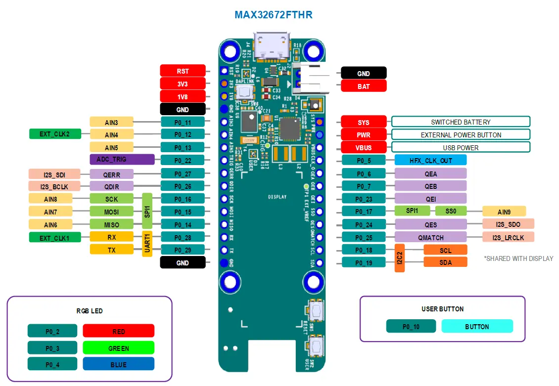
J9 Pinout
Pin |
Name |
Description |
|---|---|---|
1 |
RST |
Master Reset Signal |
2 |
3V3 |
3.3V Output. Typically used to provide 3.3V to peripherals connected to the expansion headers. |
3 |
1V8 |
1.8V Output. Typically used to provide 1.8V to peripherals connected to the expansion headers. |
4 |
GND |
Ground |
5 |
P0_11 |
GPIO or Analog Input (AIN3 channel). |
6 |
P0_12 |
GPIO or Analog Input (AIN4 channel). |
7 |
P0_13 |
GPIO or Analog Input (AIN5 channel). |
8 |
P0_22 |
GPIO or ADC_TRIG signal. |
9 |
P0_27 |
GPIO or QERR signal. |
10 |
P0_26 |
GPIO or QDIR signal. |
11 |
P0_16 |
GPIO or SPI1 clock signal. |
12 |
P0_15 |
GPIO or SPI1 MOSI signal. |
13 |
P0_14 |
GPIO or SPI1 MISO signal. |
14 |
P0_28 |
GPIO or UART1 Rx signal. |
15 |
P0_29 |
GPIO or UART1 Tx signal. |
16 |
GND |
Ground |
J7 Pinout
Pin |
Name |
Description |
|---|---|---|
1 |
SYS |
SYS Switched Connection to the Battery. This is the primary system power supply and automatically switches between the battery voltage and the USB supply when available. |
2 |
PWR |
In battery-powered mode, turns off the PMIC if shorted to ground. |
3 |
VBUS |
USB VBUS Signal. This can be used as a 5V supply when connected to USB. This pin can also be used as an input to power the board. |
4 |
P0_5 |
GPIO or HFX_CLK_OUT signal. |
5 |
P0_6 |
GPIO or QEA signal. |
6 |
P0_7 |
GPIO or QEB signal. |
7 |
P0_23 |
GPIO or QEI signal. |
8 |
P0_17 |
GPIO or SPI1 slave select signal. |
9 |
P0_24 |
GPIO or QES signal. |
10 |
P0_25 |
GPIO or QMATCH signal. |
11 |
P0_18 |
GPIO or I2C2 SCL signal. |
12 |
P0_19 |
GPIO or I2C2 SDA signal. |
Programming and Debugging
The max32672fthr board supports the runners and associated west commands listed below.
| flash | debug | rtt | attach | debugserver | |
|---|---|---|---|---|---|
| openocd | ✅ (default) | ✅ (default) | ✅ | ✅ | ✅ |
Flashing
The MAX32625 microcontroller on the board is flashed with DAPLink firmware at the factory. It allows debugging and flashing the MAX32672 Arm Core over USB.
Once the debug probe is connected to your host computer, then you can simply run the
west flash command to write a firmware image into flash. To perform a full erase,
pass the --erase option when executing west flash.
Debugging
Please refer to the Flashing section and run the west debug command
instead of west flash.