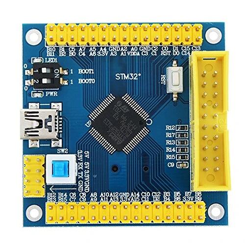
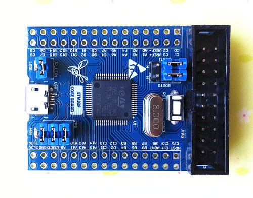
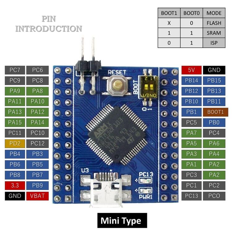
STM32F103 Mini
Overview
The STM32F103_MINI board features an ARM Cortex-M3 based STM32F103RC MCU
with a wide range of connectivity support and configurations. There are
multiple version of this board like stm32f103_mini.


Hardware
STM32F103 Mini provides the following hardware components:
STM32 microcontroller in QFP64 package
Flexible board power supply:
USB VBUS or external source (3.3V, 5V, 7 - 12V)
Power management access point
Two LEDs:
User LED (LD1), power LED (LD2)
USB re-enumeration capability:
Mass storage
More information about STM32F103RC can be found here:
Supported Features
The stm32f103_mini board supports the hardware features listed below.
- on-chip / on-board
- Feature integrated in the SoC / present on the board.
- 2 / 2
-
Number of instances that are enabled / disabled.
Click on the label to see the first instance of this feature in the board/SoC DTS files. -
vnd,foo -
Compatible string for the Devicetree binding matching the feature.
Click on the link to view the binding documentation.
stm32f103_mini/stm32f103xe target
Type |
Location |
Description |
Compatible |
|---|---|---|---|
CPU |
on-chip |
ARM Cortex-M3 CPU1 |
|
ADC |
on-chip |
||
CAN |
on-chip |
STM32 CAN controller1 |
|
Clock control |
on-chip |
STM32 RCC (Reset and Clock controller)1 |
|
on-chip |
STM32 HSE Clock1 |
||
on-chip |
|||
on-chip |
STM32F1 Main PLL for low-, medium-, high- and XL-density devices1 |
||
on-chip |
STM32F1 Microcontroller Clock Output (MCO)1 |
||
Counter |
on-chip |
STM32 counters8 |
|
DAC |
on-chip |
STM32 family DAC1 |
|
DMA |
on-chip |
STM32 DMA controller (V2bis) for the stm32F0, stm32F1 and stm32L1 soc families2 |
|
Flash controller |
on-chip |
STM32 Family flash controller1 |
|
GPIO & Headers |
on-chip |
STM32 GPIO Controller7 |
|
I2C |
on-chip |
||
Interrupt controller |
on-chip |
ARMv7-M NVIC (Nested Vectored Interrupt Controller)1 |
|
on-chip |
STM32 External Interrupt Controller1 |
||
LED |
on-board |
Group of GPIO-controlled LEDs1 |
|
MTD |
on-chip |
STM32 flash memory1 |
|
PHY |
on-chip |
This binding is to be used by all the usb transceivers which are built-in with USB IP1 |
|
Pin control |
on-chip |
STM32F1 Pin controller1 |
|
Power management |
on-chip |
STM32 power controller1 |
|
PWM |
on-chip |
||
Reset controller |
on-chip |
STM32 Reset and Clock Control (RCC) Controller1 |
|
RTC |
on-chip |
STM32 RTC1 |
|
Sensors |
on-chip |
STM32 quadrature decoder5 |
|
on-chip |
STM32 Internal Temperature Sensor1 |
||
Serial controller |
on-chip |
||
on-chip |
STM32 UART2 |
||
SMbus |
on-chip |
STM32 SMBus controller2 |
|
SPI |
on-chip |
||
Timer |
on-chip |
ARMv7-M System Tick1 |
|
on-chip |
|||
USB |
on-chip |
STM32 USB controller1 |
|
Watchdog |
on-chip |
STM32 watchdog1 |
|
on-chip |
STM32 system window watchdog1 |
Connections and IOs
Each of the GPIO pins can be configured by software as output (push-pull or open-drain), as input (with or without pull-up or pull-down), or as peripheral alternate function. Most of the GPIO pins are shared with digital or analog alternate functions. All GPIOs are high current capable except for analog inputs.
Board connectors:

Default Zephyr Peripheral Mapping:
UART_1 TX/RX: PA9/PA10
UART_2 TX/RX: PA2/PA3 (ST-Link Virtual COM Port)
SPI1 NSS/SCK/MISO/MOSI: PA4/PA5/PA6/PA7
SPI2 NSS/SCK/MISO/MOSI: PB12/PB13/PB14/PB15
I2C1 SDA/SCL: PB9/PB8
PWM1_CH1: PA8
USER_PB: PC13
LD1: PA5
USB_DC DM/DP: PA11/PA12
System Clock
The on-board 8MHz crystal is used to produce a 72MHz system clock with PLL.
Programming and Debugging
The stm32f103_mini board supports the runners and associated west commands listed below.
| flash | debug | debugserver | reset | rtt | attach | |
|---|---|---|---|---|---|---|
| jlink | ✅ | ✅ | ✅ | ✅ | ✅ | ✅ |
| openocd | ✅ (default) | ✅ (default) | ✅ | ✅ | ✅ |
Applications for the stm32f103_mini board configuration can be built and
flashed in the usual way (see Building an Application and
Run an Application for more details).
Flashing
There are 2 main entry points for flashing STM32F1X SoCs, one using the ROM bootloader, and another by using the SWD debug port (which requires additional hardware such as ST-Link). Flashing using the ROM bootloader requires a special activation pattern, which can be triggered by using the BOOT0 pin.
Flashing an application to stm32f103 mini
Here is an example for the Blinky application.
# From the root of the zephyr repository
west build -b stm32f103_mini samples/basic/blinky
west flash
You will see the LED blinking every second.
Debugging
You can debug an application in the usual way. Here is an example for the Blinky application.
# From the root of the zephyr repository
west build -b stm32f103_mini samples/basic/blinky
west debug