MEC17xxEVB ASSY6941
Overview
The MEC5 Assembly 6941 EVB kit is a development platform to evaluate the Microchip MEC174x and MEC175x series microcontrollers. This board requires a CPU daughter card: DC 176WFBGA DC ASSY 6949 for MEC1743-QLJ or MEC1753-QLJ (176-pin package) DC 176WFBGA DC ASSY 6946 for MEC1743-QSZ, MEC1753-QSZ, or MEC1653B-NSZ (144-pin package)
Hardware
MEC174x-QLJ/QSZ or MEC175x-QLJ/QSZ ARM Cortex-M4F Processor
480 KB total SRAM (416 KB code, 64 KB data) and 128 KB boot ROM
MEC1653B-NSZ ARM Cortex-M4 Processor (No FPU)
416 KB total SRAM (352 KB code, 64 KB data) and 128 KB boot ROM with PQC.
Keyboard interface
ADC & GPIO headers
Four DB9 UART connectors
FAN0, FAN1, FAN2 headers
FAN PWM interface
JTAG/SWD, ETM and MCHP Trace ports
PECI interface 3.0
I2C voltage translator
10 SMBUS headers
VCI interface
Two Hardware Driven PS/2 Port
eSPI header
2 Sockets for SPI NOR chips
One reset and VCC_PWRDGD pushbuttons
One external PCA9555 I/O port with jumper selectable I2C address.
One external LTC2489 delta-sigma ADC with jumper selectable I2C address.
Board power jumper selectable from +5V 2.1mm/5.5mm barrel connector or USB Micro A connector.
MEC175x/MEC165xB have one I3C Host controller and one I3C secondary controller each with multiple ports.
For more information about the MEC174x please see MEC174x Data Brief [1] For more information about the MEC175x please see MEC175x Data Brief [2] For more information about the MEC165xB please see MEC165xB Data Brief [3]
Supported Features
The mec_assy6941 board supports the hardware features listed below.
- on-chip / on-board
- Feature integrated in the SoC / present on the board.
- 2 / 2
-
Number of instances that are enabled / disabled.
Click on the label to see the first instance of this feature in the board/SoC DTS files. -
vnd,foo -
Compatible string for the Devicetree binding matching the feature.
Click on the link to view the binding documentation.
mec_assy6941/mec1653b_nsz target
On-target memory for this board target: 62 KiB of RAM, 352 KiB of Flash.
Type |
Location |
Description |
Compatible |
|---|---|---|---|
CPU |
on-chip |
ARM Cortex-M4 CPU1 |
|
Cryptographic accelerator |
on-chip |
Microchip XEC symmetric crypto (AES/Hash) accelerator1 |
|
GPIO & Headers |
on-chip |
Microchip CEC/MEC GPIO6 |
|
Input |
on-chip |
Microchip XEC keyboard matrix controller1 |
|
Interrupt controller |
on-chip |
ARMv7-M NVIC (Nested Vectored Interrupt Controller)1 |
|
Memory controller |
on-chip |
Microchip, XEC family Battery Backed RAM node1 |
|
MTD |
on-chip |
Microchip on-chip EEPROM1 |
|
Pin control |
on-chip |
Microchip XEC Pin Controller1 |
|
RTC |
on-chip |
Microchip XEC basic timer6 |
|
on-chip |
Microchip XEC RTC timer1 |
||
Serial controller |
on-chip |
Microchip XEC UART1 |
|
SRAM |
on-chip |
Generic on-chip SRAM1 |
|
Timer |
on-chip |
ARMv7-M System Tick1 |
|
on-chip |
Microchip XEC RTOS timer1 |
mec_assy6941/mec1743_qlj target
On-target memory for this board target: 62 KiB of RAM, 416 KiB of Flash.
Type |
Location |
Description |
Compatible |
|---|---|---|---|
CPU |
on-chip |
ARM Cortex-M4 CPU1 |
|
Cryptographic accelerator |
on-chip |
Microchip XEC symmetric crypto (AES/Hash) accelerator1 |
|
GPIO & Headers |
on-chip |
Microchip CEC/MEC GPIO6 |
|
Input |
on-chip |
Microchip XEC keyboard matrix controller1 |
|
Interrupt controller |
on-chip |
ARMv7-M NVIC (Nested Vectored Interrupt Controller)1 |
|
Memory controller |
on-chip |
Microchip, XEC family Battery Backed RAM node1 |
|
MTD |
on-chip |
Microchip on-chip EEPROM1 |
|
Pin control |
on-chip |
Microchip XEC Pin Controller1 |
|
RTC |
on-chip |
Microchip XEC basic timer6 |
|
on-chip |
Microchip XEC RTC timer1 |
||
Serial controller |
on-chip |
Microchip XEC UART1 |
|
SRAM |
on-chip |
Generic on-chip SRAM1 |
|
Timer |
on-chip |
ARMv7-M System Tick1 |
|
on-chip |
Microchip XEC RTOS timer1 |
mec_assy6941/mec1743_qsz target
On-target memory for this board target: 62 KiB of RAM, 416 KiB of Flash.
Type |
Location |
Description |
Compatible |
|---|---|---|---|
CPU |
on-chip |
ARM Cortex-M4 CPU1 |
|
Cryptographic accelerator |
on-chip |
Microchip XEC symmetric crypto (AES/Hash) accelerator1 |
|
GPIO & Headers |
on-chip |
Microchip CEC/MEC GPIO6 |
|
Input |
on-chip |
Microchip XEC keyboard matrix controller1 |
|
Interrupt controller |
on-chip |
ARMv7-M NVIC (Nested Vectored Interrupt Controller)1 |
|
Memory controller |
on-chip |
Microchip, XEC family Battery Backed RAM node1 |
|
MTD |
on-chip |
Microchip on-chip EEPROM1 |
|
Pin control |
on-chip |
Microchip XEC Pin Controller1 |
|
RTC |
on-chip |
Microchip XEC basic timer6 |
|
on-chip |
Microchip XEC RTC timer1 |
||
Serial controller |
on-chip |
Microchip XEC UART1 |
|
SRAM |
on-chip |
Generic on-chip SRAM1 |
|
Timer |
on-chip |
ARMv7-M System Tick1 |
|
on-chip |
Microchip XEC RTOS timer1 |
mec_assy6941/mec1753_qlj target
On-target memory for this board target: 62 KiB of RAM, 416 KiB of Flash.
Type |
Location |
Description |
Compatible |
|---|---|---|---|
CPU |
on-chip |
ARM Cortex-M4 CPU1 |
|
Cryptographic accelerator |
on-chip |
Microchip XEC symmetric crypto (AES/Hash) accelerator1 |
|
GPIO & Headers |
on-chip |
Microchip CEC/MEC GPIO6 |
|
Input |
on-chip |
Microchip XEC keyboard matrix controller1 |
|
Interrupt controller |
on-chip |
ARMv7-M NVIC (Nested Vectored Interrupt Controller)1 |
|
Memory controller |
on-chip |
Microchip, XEC family Battery Backed RAM node1 |
|
MTD |
on-chip |
Microchip on-chip EEPROM1 |
|
Pin control |
on-chip |
Microchip XEC Pin Controller1 |
|
RTC |
on-chip |
Microchip XEC basic timer6 |
|
on-chip |
Microchip XEC RTC timer1 |
||
Serial controller |
on-chip |
Microchip XEC UART1 |
|
SRAM |
on-chip |
Generic on-chip SRAM1 |
|
Timer |
on-chip |
ARMv7-M System Tick1 |
|
on-chip |
Microchip XEC RTOS timer1 |
mec_assy6941/mec1753_qsz target
On-target memory for this board target: 62 KiB of RAM, 416 KiB of Flash.
Type |
Location |
Description |
Compatible |
|---|---|---|---|
CPU |
on-chip |
ARM Cortex-M4 CPU1 |
|
Cryptographic accelerator |
on-chip |
Microchip XEC symmetric crypto (AES/Hash) accelerator1 |
|
GPIO & Headers |
on-chip |
Microchip CEC/MEC GPIO6 |
|
Input |
on-chip |
Microchip XEC keyboard matrix controller1 |
|
Interrupt controller |
on-chip |
ARMv7-M NVIC (Nested Vectored Interrupt Controller)1 |
|
Memory controller |
on-chip |
Microchip, XEC family Battery Backed RAM node1 |
|
MTD |
on-chip |
Microchip on-chip EEPROM1 |
|
Pin control |
on-chip |
Microchip XEC Pin Controller1 |
|
RTC |
on-chip |
Microchip XEC basic timer6 |
|
on-chip |
Microchip XEC RTC timer1 |
||
Serial controller |
on-chip |
Microchip XEC UART1 |
|
SRAM |
on-chip |
Generic on-chip SRAM1 |
|
Timer |
on-chip |
ARMv7-M System Tick1 |
|
on-chip |
Microchip XEC RTOS timer1 |
Connections and IOs
This evaluation board kit is comprised of the following HW blocks:
MEC174x EVB ASSY 6941 Rev B
MEC174x 176WFBGA SOLDER DC ASSY 6942 with MEC1743Q-LJ or MEC1753Q-LJ silicon
SPI DONGLE ASSY 6791
System Clock
The MEC174x/MEC175x MCU is configured to use the 96Mhz internal oscillator with the on-chip PLL to generate a resulting EC clock rate of 96 MHz. See Processor clock control register in chapter 4 “4.0 POWER, CLOCKS, and RESETS” of the data sheet in the references at the end of this document.
Serial Port
UART1 is configured for serial logs.
Jumper settings
Please follow the jumper settings below to properly demo this board. Advanced users may deviate from this recommendation.
Jumper settings for EVB Assy 6941 Rev B
Boot-ROM Straps
These jumpers configure MEC174x/MEC175x Boot-ROM straps.
JP1 1-2UART_BSTRAP Normal Boot
JP2 1-2CR_STRAP Normal Boot
JP3 2-3JTAG_STRAP JTAG/SWD interface is not held in reset
JP4 2-3CMP_STRAP GPIO207 is available as a GPIO
JP5 1-2PWRGD_STRAP
JP7 1-2BSS_STRAP Select eSPI CAF vs G3 if enabled in OTP
JP8 1-2BSS_STRAP Default BSS_STRAP. Select load from Shared SPI
JP6 1-2VTR2_STRAP
JP9 1-2CRISIS_RECOVERY_STRAP
Peripheral Routing Jumpers
UART0 to P19A DB9(top)
JP89 No jumperRS-232 transceiver U8 not in reset.
JP21 2-3, 8-9Select UART0_TX and UART0_RX from GPIOs.
JP22 1-2, 4-5Select UART0_TX and UART0_RX to U8.
UART1 to P19B DB9(bottom)
JP90 No jumperRS-232 transceiver U9 not in reset.
JP91 1-2, 4-5Connect UART1_TX and UART1_RX to U9.
JP24 2-3, 5-6Select UART1_TX and UART1_RX from GPIOs.
Shared SPI on J18 2x10 header.
JP18 14-15Select SHD_nCS0.
JP18 17-18Select SHD_CLK.
JP18 2-3Select SHD_IO0.
JP18 5-6Select SHD_IO1.
JP18 8-9Select SHD_IO2(nWP).
JP18 11-12Select SHD_IO3(nHOLD).
- Second chip select for accessing SPI dongle flash U7.
JP18 20-12Select SHD_nCS1.
JTAG/SWD ARM JTAG 2x10 J29.
JP80 1-2No jumper. This jumper holds JTAG/SWD interface in reset.
JP12 2-3Select JTAG_TDO or SWO.
JP12 5-6Select JTAG_TDI Not required for ARM SWD.
JP12 8-9Select JTAG_TMS or SWDIO.
JP12 11-12Select JTAG_CLK or SWCLK.
NOTE: ARM SWD is a two pin interface using JTAG_TMS as a bidirectional I/O pin and JTAG_CLK. The ARM Serial Wire Output Trace feature is on a third pin, JTAG_TDO. Configuration options are:
4-pin JTAG or SWD plus SWO. Connect all four JP12 jumpers shown above.
2-pin SWD plus SWO. Connect JP12 jumpers for JTAG_TDO, JTAG_TMS, and JTAG_CLK. JTAG_TDI is available to use as GPIO145.
2-pin SWD only. Connect JP12 jumpers for JTAG_TMS and JTAG_CLK. JTAG_TDI and JTAG_TDO are available as GPIO145 and GPIO146 respectively
Jumper settings for MEC174x/MEC175x 176WFBGA Socket DC Assy 6942 Rev A0p1
The jumper configuration explained above covers the base board. The ASSY
6942 MEC174x/MEC175x CPU board provides capability for an optional, external 32KHz
clock source. The card includes a 32KHz crystal oscillator. The card can
also be configured to use an external 50% duty cycle 32KHz source on the
XTAL2/32KHZ_IN pin. Note, firmware must set the MEC174x/MEC175x clock enable
register to select the external source matching the jumper settings. If
using the MEC174x/MEC175x internal silicon oscillator then the 32K jumper settings
are don’t cares. JP1 on DC is for scoping test clock outputs. Please
refer to the schematic in reference section below.
Parallel 32KHz crystal configuration
JP1 1x2 ON
JP2 1x3 2-3
External 32KHz 50% duty cycle configuration
JP1 1x2 NC
JP2 1x3 1-2
NOTE: EVB JP117 3-4 Connects 32KHz OSC U15 output to DC.
Building
Build :zephyr:code-sample:’hello_world` application as you normally do.
The file
spi_image.binwill be created if the build system can find the image generation tool. This binary image can be used to flash the SPI chip.
Programming and Debugging
Setup
Example programming the SPI flash on the Assy6791 SPI dongle.
We use a low cost USB-to-GPIO device based on the FTDI FT232H device.
The FT232H device used here is the AdaFruit FT232H [6] The AdaFruit FT232H supports both 5V and 3.3V parts.
The linux flashrom tool supports FT232H USB-to-GPIO used as an SPI programmer.
$ sudo /usr/sbin/flashrom -V -p ft2232_spi:type=232H,divisor=30 -w spi_image.bin
Clone the MEC174x SPI Image Gen [4] or MEC175x SPI Image Gen [5] repository or download the files within that directory.
Make the image generation available for Zephyr, by making the tool searchable by path, or by setting an environment variable
MEC5_SPI_GEN, for example:export MEC5_SPI_GEN=<path to tool>/mec174x_spi_gen_linux_x86_64 or export MEC5_SPI_GEN=<path to tool>/mec175x_spi_gen_linux_x86_64
The default configuration file is mec174x_spi_cfg.txt or mec175x_spi_cfg.txt located in ${BOARD_DIR}/support. If needed, a custom SPI image configuration file can be specified to override the default one.
export MEC5_SPI_CFG=custom_spi_cfg.txt
Wiring
Connect the SPI Dongle ASSY 6791 to
J18in the EVB.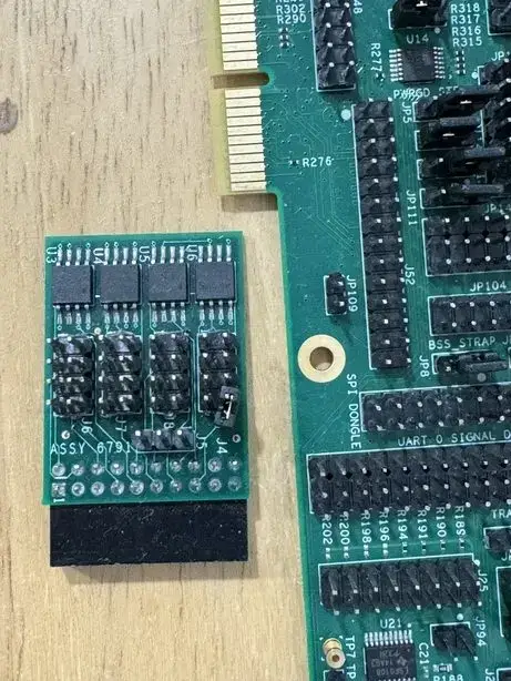
IMPORTANT: Temporarily remove the jumper from JP87 to isolate SPI dongle power from EVB power rails. This will prevent the SPI programmer from back driving voltage to the EVB.
Connect programmer to the header J6 on the Assy6791 board, it will flash the SPI NOR chip
U3.Note
The AdaFruit FT232H board supports +5V or +3.3V SPI flash devices. It has separate +3V and +5V pins. You should connect the appropriate voltage rail to the Assy6791 flash dongle’s J6-1 power pin. It is recommended to remove the Assy6791 dongle from the EVB when flashing. If the dongle is attached to an unpowered EVB then then the SPI programmer will back drive all the components. Back driving voltage can be avoided by removing the jumper on EVB JP87 disconnecting VTR1/VTR2 from the 2x10 header J18.
AdaFruit Connector
Assy6791 J6 Connector
3V or 5V
1
GND
2
D3
3
D0
4
D2
6
D1
5
The AdaFruit FT232H has USB type-C connector. Connect it to your development system with the appropriate USB cable. The FT232H board and Assy6791 dongle will be powered.
Flashing
Run your favorite terminal program
Flash the SPI image created by Microchip SPI image generator during the zephyr build process. The divisor option flashrom passes to the linux FT232 driver divides down the 60 MHz SPI clock. You can read the current SPI image by changing the ‘-w’ option to ‘-r’.
$ sudo /usr/sbin/flashrom -V -p ft2232_spi:type=232H,divisor=30 -w spi_image.bin
When flashrom completes. Disconnect USB cable to remove power from the AdaFruit FT232H programmer. Disconnect FT232H from Assy6791 dongle. Replace the jumper on EVB JP87.
# Power on the EVB.
You should see
"Hello World! <board name>"in the first terminal window. If you don’t see this message, press the Reset button and the message should appear.
Debugging
This board comes with a Cortex ETM port which facilitates tracing and debugging using a single physical connection. In addition, it comes with sockets for JTAG only sessions.
Troubleshooting
In case you don’t see your application running, please make sure
LED1andLED2are lit. If one of these is off, then check the power-related jumpers again.If you suspect the SPI image was not programmed remove the SPI dongle from the EVB and try flashing it again.
PCA9555 Enabling
To enable PCA9555PW and test the I2C on mec172xevb_assy6906, additional works are needed:
As the I2C slave device NXP pca95xx on mec172xevb_assy6906 is connected to I2C00 port, however, I2C00 port is shared with UART2 RS232 to TTL converter used to catch serial log, so it’s not possible to use UART2 and I2C00 port simultaneously. We need to change to use I2C01 port by making some jumpers setting as below:
Pin 1
Pin 2
Comment
JP49.1
JP49.2
Connect PCA9555 VCC to +3.3V_STBY
JP53.1
JP53.2
Select address 0100b, which means 0x26
JP12.13
JP12.14
Connect I2C01_SDA from CPU to header J20
JP12.4
JP12.5
Connect I2C01_SCL from CPU to header J20
JP77.7
JP77.8
External pull-up for I2C01_SDA
JP77.9
JP77.10
External pull-up for I2C01_SCL
JP58.1
JP20.1
Connect NXP PCA9555 SCL to I2C01
JP58.3
JP20.3
Connect NXP PCA9555 SDA to I2C01